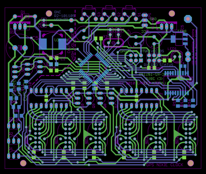
General Principle of PCB Layout

Layout is an important part in the design of PCB.The layout of the design will directly affect the effect of wiring, so it can be considered reasonable layout is the first step in the success of PCB design.The layout of the way is divided into two kinds, one is interactive layout, the other is automatic layout. And the automatic is the most used one.
In the PCB layout, the first consideration is the size of the PCB.The bigger the PCB size, the higher the impedance, the ability to resist the noise, and the cost will be increased; The smaller the size, the worse the heat dissipation, and the adjacent circuit is vulnerable to be interfered.
The second consideration is the size of the PCB. After determining the size of the PCB, need to determine the location of special components. Finally, according to the functional unit, considerate the layout of all the components in the circuit.
The following principles need to be followed in the determination of special components:
(1). Shorten the length of the connection between FM components as far as possible. Vulnerable components can not be too close to each other, and input components and output components should be far away from each other.
(2). There may be a high potential difference between certain components or wires, should increase the distance between them, to avoid accidental short-circuit caused an accident. The components with strong electric should be arranged in the position where body is not easy to reach.
(3). Components of more than 15g weight shall be fixed by the bracket, and then welded. The components which large and heavy, and large calorific value are not fit for the PCB.
(4). For the potentiometer, adjustable inductor coil, variable capacitor, micro switch, such as the layout of the components should be considered the structural requirements of the whole machine.
(5). Should be set aside for the location of the positioning hole and the fixed bracket in PCB design.
The following principles need to be followed in the layout circuit and the functional unit:
(1). According to the location of each functional unit in the circuit, the layout is convenient for the signal to circulate, and the signal can be kept in the same direction as possible.
(2). To each functional unit of the core components as the center, around them to layout. Components should be arranged in PCB board uniformly, neatly, compactly. And try to reduce and shorten the connection between the various components of the lead.
(3). For frequency modulation circuit, the distribution parameters of the components should be considered. General circuits should be made as far as possible to parallel arrangement of components. Thus, not only beautiful, but also easy to weld, and easy to mass production.
(4). About the components located at the edge of PCB, the distance between them should not less than 2mm. When the size of PCB board more than 200mm*150mm, should consider: the Mechanical Strength of PCB board.
About Suntek
Suntek is the established leader in providing innovative and reliable PCB & PCBA solutions for the electronic design industry. With over 10 years of experience in supplying high quality, on-time PCB & PCBA prototypes and mass production,Suntek is committed to improving production process for the design engineer from quote to delivery.Suntek provides unparalleled customer service and leads the industry with a real On-Time Guarantee that is the first of its kind. For more information about Suntek's innovative PCB & PCBA solutions, or to learn more about quote and ordering process, please visit http://www.suntek-electronics.com

